3.1 Starting the Simulator
The simultor controls can be accessed either via the "Simulate" menu,
or the button bar. Start a simulation by selecting "Begin Simulation"
from the "Simulate" menu, or by pressing the "play" button on the
button bar. A scope trace window will appear when you start the
simulator, as well as text windows for any "tty" devices in your
circuit. If there are any auto execute script files (see Simulation Scripts for details) these will be
executed too.
The simulation will be performed with the designated root module at
the top-level. The simulator internally expands any module instances
in your circuit. Since the path you take to get to a module is
significant to the simulator, you cannot jump directly to submodules
but must "navigate" your way to them by selecting a module at the
current level and by opening it using the menu or the '>' keyboard
command. You can leave a module you are in with the '<' keyboard
command.
Gate and wire names in sub-modules are referenced by prepending a
dot-separated "path" of module instance names. For instance, suppose
there are two instances of a module named "foo" in the root module
with instance names "g1" and "g2". Now suppose the "foo" module
contains a wire named "w1". These wire names are referenced by the
simulator as "g1.w1" and "g2.w1" to distinguish the two instances.
TkGate is an event-driven simulator. Time is measured in discrete
units called "epochs". Each gate has a delay of a certain number of
epochs. Some complex gates have multiple delay constants. In
addition, some gates such as registers and memories have additional
delay parameters which affect internal state changes.
The basic simulator commands are:
| Function |
Button |
Description |
| Run |
 |
Enters continuous simulation mode. The simulation will continue as long as there are events in
the event queue. If there are any clock gates in your circuit, this will mean the simulation will
continue indefinately. If the circuit is combinational, the simulation will continue until
the circuit reaches quiescence. |
| Pause |
 |
Causes a continuously running simulation to stop. |
| Step Epoch |
 |
Causes the simulation to advance a fixed number of epochs. The number of
epochs to advance can be set on the simulation options menu. You can also
invoke this command with the spacebar.
|
| Step Cycle |
 |
Causes the simulation to advance to the rising edge of a clock.
You can set the number of clock cycles to simulate and the number of
epochs past the designated cycle to step (to allow time for registers
to change value). The default is to trigger on any clock, but you can
designate a specific clock in the simulator options menu.
You can also invoke this command with the tab key.
|
| End Simulation |
 |
Causes the simulation to be terminated and all probes to be deleted. |
Other simulator commands will be discussed in the following sections.
3.2 Simulator Options
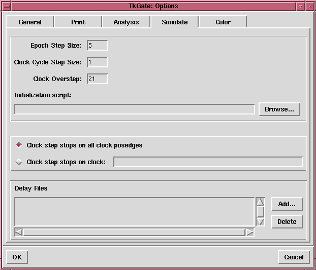 Several simulation options can be set through the options dialog box.
To edit the simulator options, select "Options..." from the "File"
menu, and then select the "Simulator" tab from the tab box.
Several simulation options can be set through the options dialog box.
To edit the simulator options, select "Options..." from the "File"
menu, and then select the "Simulator" tab from the tab box.
The simulator options are:
- Epoch Step Size: Specifies the number of epochs to step each time the
simulator is stepped by using the step button or by pressing the space bar.
- Clock Cycle Step Size: Specifies the number of clock cycles
to step each time the clock is stepped by using the clock step button or by
pressing the tab key.
- Clock Overstep: Specifies the number of epochs to simulate
past the clock edge when doing a clock step. This can be used to
advance the simulator enough for registers to change value.
- Initialization Script: Specifies a simulation script to
automatically execute when starting the simulator. The script file
specified here is a global property and applys to any circuit that has
been loaded into TkGate. To specify scripts specific to a particular
circuit see circuit initalization
scripts.
- Clock step stops on all clock posedges: Indicates that the
clock step command should trigger on positive edges on all clocks in the
circuit as.
- Clock step stops on clock: Indicates that the clock step
command should trigger on positive edges only on the specified clock.
This option is only useful for circuits with multiple clocks.
- Delay Files: Specifies additional files from which to load
gate delay specifications. More on writting gate delay specifications
can be found in Gate Delay Files
3.3 Observing the Output
Except when otherwise noted, verilog syntax is used to specify and
display values. A Verilog syntax number contains a prefix to specify
the bit width, a quote character, a radix character and the digits of
the number. The radix characters using in TkGate are "b" for binary,
and "h" for hexidecimal. For example "8'h3e" is the 8-bit hexidecimal
number "3e".
The simulator supports the following logic values:
Symbol |
Scope |
Description |
| 0 |
 |
Logic 0 |
| 1 |
 |
Logic 1 |
| x |
 |
Unknown |
| z |
 |
Floating |
| L |
 |
Low (the signal is either floating or zero) |
| H |
 |
High (the signal is either floating or one) |
 To display the value of a signal in a circuit, click and hold the
mouse button on a wire. This will display the current value driven on
the wire in verilog syntax. The value will disappear when you release
the mouse button. This feature can be used both when the simulator is
paused and when it is in continuous simulation mode. When the
simulator is in continuous simulation mode, the value displayed will
be the value at the time the mouse button was first pressed.
To display the value of a signal in a circuit, click and hold the
mouse button on a wire. This will display the current value driven on
the wire in verilog syntax. The value will disappear when you release
the mouse button. This feature can be used both when the simulator is
paused and when it is in continuous simulation mode. When the
simulator is in continuous simulation mode, the value displayed will
be the value at the time the mouse button was first pressed.
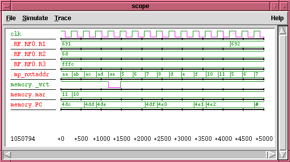 To set a permanent probe on a signal, double click on a wire. This
will add or remove a probe. When a probe is set on a wire, its value
will be continuously displayed in the scope window. The values of
multi-bit signals will be displayed as hex numbers.
To set a permanent probe on a signal, double click on a wire. This
will add or remove a probe. When a probe is set on a wire, its value
will be continuously displayed in the scope window. The values of
multi-bit signals will be displayed as hex numbers.
To change the range of values displayed and the scale of the display
you can use the scrollbar, the mouse, or keyboard commands. Moving
the scrollbar will set the range relative to the entire simulation
run. You can get more fine grain control by clicking in the trace
window with the left mouse button and dragging the trace left or
right. To zoom in, you can either press the left mouse button while
holding the shift key, or press the '>' key. To zoom out, you can
either press the right mouse button while holding the shift key, or
press the '<' key.
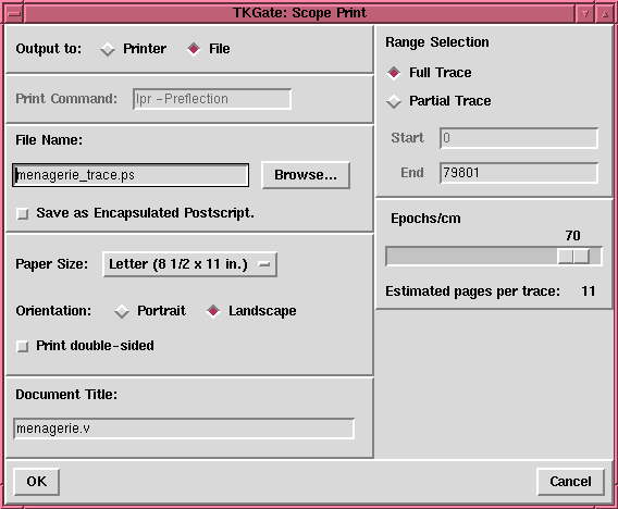 To print a scope trace, choose the "Print..." option from the "File"
menu on the scope window, or use the keyboard shortcut "Ctl-s p". The
dialog box shown here will be displayed. The left half of the dialog
box is the same as the left half of the dialog box used to print circuits. The
right half includes options for selecting the time range to print and
the scale factor to use. Beware that simulation traces can grow very
large, very quickly, especially when you use the continuous simulation
mode. An estimate of the number of pages needed for each trace you
have set is displayed to help you set parameters.
To print a scope trace, choose the "Print..." option from the "File"
menu on the scope window, or use the keyboard shortcut "Ctl-s p". The
dialog box shown here will be displayed. The left half of the dialog
box is the same as the left half of the dialog box used to print circuits. The
right half includes options for selecting the time range to print and
the scale factor to use. Beware that simulation traces can grow very
large, very quickly, especially when you use the continuous simulation
mode. An estimate of the number of pages needed for each trace you
have set is displayed to help you set parameters.
3.4 Controlling the Input
There are three types of circuit elements which can be used to control
your circuit: the single-bit switch, the multi-bit dip switch and the
tty.
3.4.1 Switches and Dip Switches
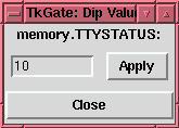 Switches can be manipulated by simply clicking on them to toggle their
values. To change a dip switch value, click on the dip switch to open
a dialog box for setting that dip switch. Enter a value in the entry
area, and press the apply button to set the switch. The dialog box will
remain until you hit close.
Switches can be manipulated by simply clicking on them to toggle their
values. To change a dip switch value, click on the dip switch to open
a dialog box for setting that dip switch. Enter a value in the entry
area, and press the apply button to set the switch. The dialog box will
remain until you hit close.
3.4.2 Ttys
The third type of input element is the tty. The tty is actually both
an input and an output device modeling an interactive terminal. When
you start the simulator, one tty window will appear for each instance
of a tty gate in your circuit. Your circuit can send characters to
and receive characters from the tty gate.
To send a character to a tty element, drive the RD input with the
ascii code of the character to transmit and wait for the DTR output to
go high. Next assert the DSR signal (positive high). The character
will be transmitted on the positive edge of the DSR signal. You must
then unassert the DSR signal so that the next character can be sent.
To receive a character, first unassert the CTS signal and wait for the
RTS signal to go high. You can then read the value on the TD ouput of
the tty. Once you have read the value, assert the CTS signal to
indicate that you have received the character.
3.5 Setting Breakpoints
| Button |
|---|
 |
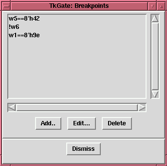 Breakpoints can be used to set conditions which will cause a
continuously running simulation to pause. To display the breakpoint
dialog box, choose the "Breakpoint..." option from the "Simulate"
menu. This will cause the breakpoint editor such as then one shown to
the right to be displayed. You can use the button to add, edit or
delete breakpoints.
Breakpoints can be used to set conditions which will cause a
continuously running simulation to pause. To display the breakpoint
dialog box, choose the "Breakpoint..." option from the "Simulate"
menu. This will cause the breakpoint editor such as then one shown to
the right to be displayed. You can use the button to add, edit or
delete breakpoints.
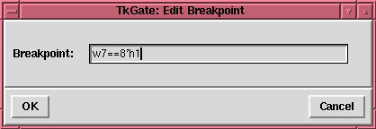
When you add or edit a breakpoint, a breakpint editing dialog box such
as the one shown here will be displayed. Enter or edit the breakpoint
condition and hit OK. Currently, only a limited number of breakpoint
types can be used. Only a single signal can be compared with a
constant using a single relational operator. The relational operators
are the standard relational operators used in C. The value must be a
verilog syntax constant. Alternitively, you
can simply type a signal name to break when the signal becomes
non-zero, or a signal name prepended with the '!' operator to break
when the signal becomes zero.
3.6 Initializing Memories
A circuit can contain one or more memories (ROM and RAM gates). You
can initialize memories from a file, or dump the contents of a memory
to a file. Use the options in the table below to load or dump
memories.
| Function |
Button |
Description |
| Load Memory... |
 |
Load memories from the selected file. If a memory gate is selected, that memory
will be the default memory to load. If the memory file contains one or more "memory" keywords,
the specified memory(ies) will be loaded with the contents of the file. When loading a file,
the current directory, the directory of the current circuit file, and the user's home directory
will be searched. |
| Dump Memory... |
 |
Dumps the contents of the selected memory to a file. |
Memory files have the extension ".mem" be default. A memory file is
composed of a number of lines. Blank lines and lines begining with
'#' are ignored. Other lines must be a "memory" declaration or an
address in hexidecimal followed by a slash, and a list of memory
values in hexadecimal. An example memory file might look like:
100/ e1 f0 0 0 e1 e0 0 0
108/ 81 0 0 0 12 1 bd 0
110/ e 1 e1 d0 dc 7 85 0
118/ 6f 6 81 0 0 0 4e 4
120/ 69 f0 2 0 85 0 64 0
128/ 81 0 0 0 26 4 69 f0
130/ 2 0 ed 0 60 6 62 6
138/ ed 0 5e 6 1 0 85 0
The address at the beginning of the line specifies the address at
which to begin storing values. Values are stored sequentially from
the specified address one word at a time for the rest of the line.
If there is no "memory" keyword in the memory file, the selected
memory gate will be loaded. The memory keyword requires a single
argument specifing the name of a memory. For example:
memory memory.m1
100/ e1 f0 0 0 e1 e0 0 0
108/ 81 0 0 0 12 1 bd 0
will load the memory "m1" in the instance named "memory" which is a
submodule of the root module. In order to assist in creating memory
files, you can use gmac to compile
microcode and macrocode descriptions into TkGate-compatable memory
files.
For RAM memories, the contents of the loaded memory are frozen until
first time the write line transitions to a stable value (logic 0 or
1). This prevents the data loaded from being destroyed due to unknown
values on the write and address lines until the circuit has time to
intitilize these signals.
3.7 Simulation Scripts
| Button |
|---|
 |
Simulation scripts can be used to perform most of the operations you
can do manually. You can set and remove probes, change switch values,
load memories, set breakpoints, and step and start/stop the simulator.
Simulation script are useful for setting up a simulation before
starting, or for running a simulation in batch mode. You can load a
simulation script using the button on the button bar or by selecting
"Exec. Script..." from the "Simulate" menu. The default extension for
simulation scriptes is ".gss". When loading a file, the current
directory, the directory of the current circuit file, and the user's
home directory will be searched.
You can also arrange for simulation scripts to be automatically
executed when you start the simulator either by specifying a
simulation script in the simulation options
dialog box, or by adding simulation scripts as circuit options. The following
simulation script commands are recognized. Arguments specified
between "?" characters denote optional arguments.
| Command |
Description |
| include "file" |
Includes the specified file as if its contents appear here in the simulation script. |
| step n |
Steps the specified number of epochs. |
| clock(+/-) ?[name]? n ?+m? |
Step n clock steps. If the character after "clock" is a
"+" stepping will be on positive clock edges. If the character is a
"-" the stepping will be on negative clock edges. If name is
specified, only edges on that clock will be used. If m is
specified, then the simulator will step that number of epochs after
the final clock edge.
|
| run |
Put the simulator into continuous simulation mode. This command will
block until a breakpoint is hit, or until you press the pause button. |
| break ?[name]? cond |
Sets the breakpoint cond which must have the syntax
described in the section on breakpoints. If
a name is specifed in square brackets. This breakpoint will be
assigned a symbolic name which can be referenced to deleted the
breakpoint later. If no name is specified, then it will not be
possible to remove the breakpoint from a simulation script.
|
| delete [name] |
Deletes the specified breakpoint. Only breakpoints set through a
simulation script and assigned a symbolic name can be deleted. |
| set name value |
Sets the value of a switch or dip switch. Name should specify the
full path of a switch or dip switch, and value should be a
verilog syntax constant. |
| probe name |
Sets a probe on signal name. The name should be specified as a full path. |
| unprobe name |
Removes the probe on signal name. The name should be specified as a full path. |
| load ?name? "file" |
Load memories from a file. If you specify a memory name, that memory will be the default memory. |
| dump name "file" |
Dumps the contents of the specified memory to a file. |
| zoom n |
Set the zoom factor for the scope. Positive numbers increase the
displayed range and negative numbers decrease the range.
|
3.8 Using the Error Reporter
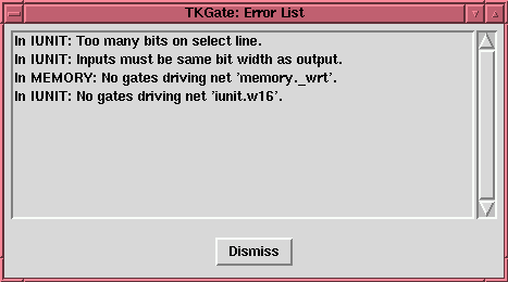 If there are any errors in the circuit when you start the simulator.
An error list box will appear with the list of errors and the modules
in which these errors occured. You can scan through the list of
errors using the "Ctl-n" and "Ctl-p" keyboard commands. TkGate will
go to the module in which the current error occured and highlight the
position of the error with an "X" symbol.
If there are any errors in the circuit when you start the simulator.
An error list box will appear with the list of errors and the modules
in which these errors occured. You can scan through the list of
errors using the "Ctl-n" and "Ctl-p" keyboard commands. TkGate will
go to the module in which the current error occured and highlight the
position of the error with an "X" symbol.
3.9 Gate Delay Files
Gate delay, area and power (power specifications are not used)
parameters can be specified through a collection of gdf (Gate Delay
File) specification files. The default file "gdf/default.gdf" in the
TkGate home directory is always loaded, but the definitions may be
replaced by loading additional delay files through the options box.
Each gate delay file should contain one or more technology blocks
having the form:
technology cmos {
  ...
}
Technology blocks implement a new set of delay parameters and the
specified technology name becomes a name that can be specified as a
technology through the "Delay" page of
the gate properties box. The body of the technology block should
consist of a set of gate primitive declarations. Each gate primitive
should be descibred in a block defining all the delay and possible
area and power parametes of the block in terms of number of inputs,
bit-widths of inputs and existence of inverters on inputs. For
example, the block for the "mux" primitive might look like:
primitive mux {
  delay<I-Z> = (2*(num(S)+1) + 2*num(I)) + 2*(inv(I) || inv(Z));
  delay<S-Z> = (2*(num(S)+1) + 2*num(I));
  area = bits(Z)*((2*(num(S)+1) + 2*num(I)) + 2*inv(I));
}
The two "delay" lines define the delay from the input to the output
(I-Z) and from the select to the output (S-Z), respectively. The area
line defines the estimated area of the gate. Expressions may include
the C-style operators "+", "-", "*", "/", "&&", "||", "==", "!=", ">", ">=", "<",
"<=", and "!", the "power of" operator "**" and
the functions listed in the table below.
| Function | Description |
|---|
| num(p) | Normally, "p" specifies a group of related
ports in which case this function returns the number of ports in the
group. For example, on an n-input AND gate with inputs I1 through In,
the expression num(I) would return n. |
| bits(p) | Returns the number of bits on the specified
port. If "p" represents a group of ports, the highest bit-width of
the group is returned. |
| inv(p) | When "p" is specific port, a 1 is returned if
there is an inverter on the port, 0 otherwise. When "p" specifies a
group of ports, the number of ports with inverters is returned.
|
| log(expr) | Returns the ceiling of the base-2 log of an expression. |
It is also possible to write procedural delay/area definitions. For example, consider
the parameter specification for the "and" primitive.
primitive and {
  delay<I-Z> = {
    if ((inv(I) == num(I)))     // Determine if an inverter is necessary.  An
      d = inv(Z);               //   inverter is not required if the output is
    else if ((inv(I) == 0))     //   inverting and all inputs are non-inverting
      d = !inv(Z);              //   (i.e., it is an AND gate), or if all inputs
    else                        //   are inverting and the output is non-inverting
      d = 1;                    //   (i.e., it is a NOR gate).

    if (num(I) == 1) {          // If one input, treat this as a reduction gate
      return 2*bits(I0) + 2*d;  //   one Tr. delay per bit plus inverter delay.
    } else {                    // If multiple inputs, treat this as a normal gate
      return 2*num(I) + 2*d;    //   one Tr. delay per input plus inverter delay.
    }
  }

  area = {
    if ((inv(I) == num(I)))     // Estimate number of inverters required.  If all
      d = inv(Z);               //   inputs are inverted, an inverter is required
    else if ((inv(I) == 0))     //   iff the output is inverted.  If all inputs
      d = !inv(Z);              //   are non-inverted, an inverter is required iff
    else                        //   the output is non-inverted.  Otherwise we need
      d = inv(I);               //   an inverter for each inverted input.

    if (num(I) == 1) {          // If one input, treat this as a reduction gate
      a = 2*bits(I0) + 2*d;	//   one Tr. per bit plus inverter Trs.
    } else {			// If multiple inputs, treat this as a normal gate
      a = 2*num(I) + 2*d;	//   one Tr. per input plus inverter Trs.
    }
    return bits(Z)*a;           // Multiply by number of bit slices.
  }
}
In a procedural specification, statements are executed sequentially
until a "return" statement sets the value for the parameter.
C-style if and switch statements may be used in
procedural specifications, but there are no looping constructs.
A technology block need not specify every single primitive type. For
example, suppose we have a technology definition for CMOS which
includes a definition for a buffer as shown here:
technology CMOS {
  primitive buf {
    delay<I-Z> = 2 + 2*(inv(I) == inv(Z));
    area = bits(Z)*(2 + 2*(inv(I) == inv(Z)));
  }
  ...rest of CMOS definition...
}
We might create a special technology definition "HP_CMOS" which
contains high-power versions of a subset of the standard CMOS gates.
In the example here, we provide a special high-power buffer that has
the delay of a standard buffer, but twice the area (and power).
/*
 * A high-power buffer with half the delay and double the area/power.
 */
technology HP_CMOS {
  primitive buf {
    delay<I-Z> =  1 + (inv(I) == inv(Z));
    area = 2*bits(Z)*(2 + 2*(inv(I) == inv(Z)));
  }
}
If you assign the technology type HP_CMOS to any gates for which there
is no primitive definition, delay values from the technology "default"
will be used.
The table below lists all of the primitive gates for which delay may
be specified and their delay parameters. The default values given are
the values for a "basic" gate created from the "Make" with no changes
to the number of inputs, input/output inverters, or bit widths of any
of the ports.
| Gate Type | Parameter | Default | Description |
|---|
| and | I-Z | 6 | Delay from input to output. |
| or | I-Z | 6 | Delay from input to output. |
| xor | I-Z | 8 | Delay from input to output. |
| buf | I-Z | 4 | Delay from input to output. |
| bufif1 | E-Z | 4 | Delay from enable to output. |
| I-Z | 6 | Delay from data input to output. |
| nmos | I-Z | 2 | Delay from data input to output. |
| G-Z | 1 | Delay from gate to output. |
| pmos | I-Z | 2 | Delay from data input to output. |
| G-Z | 1 | Delay from gate to output. |
| add | A/B-S | 68 | Delay from operand input to sum. |
| A/B-CO | 70 | Delay from operand input to carry out. |
| CI-S | 62 | Delay from carry in to sum. |
| CI-CO | 64 | Delay from carry in to carry out. |
| register | setup | 10 | Time before clock edge data-in must be stable. |
| hold | 10 | Time after clock edge data-in must remain stable. |
| CK-Q | 20 | Time from clock edge until output changes. |
| mux | S-Z | 8 | Delay from select line to output. |
| I-Z | 8 | Delay from data input to output. |
| demux | E-Z | 6 | Delay from enable line to output. |
| I-Z | 6 | Delay from data input to output. |
| mult | A/B-P | 252 | Delay from operand input to output. |
| div | A/B-Q | 236 | Delay from operand input to quotient. |
| A/B-R | 236 | Delay from operand input to remainder. |
| ram | OE-D | 10 | Delay from output enable to data-out. |
| CS-D | 10 | Delay from chip select to data out. |
| A-D | 70 | Delay from the address line to the data out. |
| addr_setup | 10 | Time before write is asserted that address must be stable. |
| data_setup | 10 | Time before write is asserted that data-in must be stable. |
| addr_hold | 10 | Time after write is unasserted that address must remain stable. |
| data_hold | 10 | Time after write is unasserted that data-in must remain stable. |
| rom | OE-D | 10 | Delay from output enable to data-out. |
| A-D | 50 | Delay from address to data-out. |
| tty | TR | 150 | Time to transmit a character. |
| RTS_UP | 2 | Time after transmition is complete before RTS line is raised. |
| RTS_DN | 8 | Time after DSR is asserted that RTS will fall. |
| RD | 150 | Time to read a character. |
| DTR_UP | 2 | Time after character is received that DTR will be raised. |
| DTR_DN | 2 | Time after CTS is asserted that DTR will fall. |
| lshift | S-Z | 16 | Delay from shift select to output. |
| I-Z | 18 | Delay from data-in to output. |
| rshift | S-Z | 16 | Delay from shift select to output. |
| I-Z | 18 | Delay from data-in to output. |
| arshift | S-Z | 16 | Delay from shift select to output. |
| I-Z | 18 | Delay from data-in to output. |
| roll | S-Z | 16 | Delay from shift select to output. |
| I-Z | 18 | Delay from data-in to output. |
3.10 Critical Path Analysis
 The TkGate simulator incorporates a circuit analyzer for critical path
analysis. Note that the current analyzer uses a simple static path
analysis algorithm and can not detect false paths. The analyzer will
find and display a list of a specified number of long delay paths in
the circuit. Only paths which are formed by finding the worst case
delay to an output and the worst case delay to an input for some
internal node are lists (i.e., all of the slack for paths shorter than
the longest is at one net).
The TkGate simulator incorporates a circuit analyzer for critical path
analysis. Note that the current analyzer uses a simple static path
analysis algorithm and can not detect false paths. The analyzer will
find and display a list of a specified number of long delay paths in
the circuit. Only paths which are formed by finding the worst case
delay to an output and the worst case delay to an input for some
internal node are lists (i.e., all of the slack for paths shorter than
the longest is at one net).
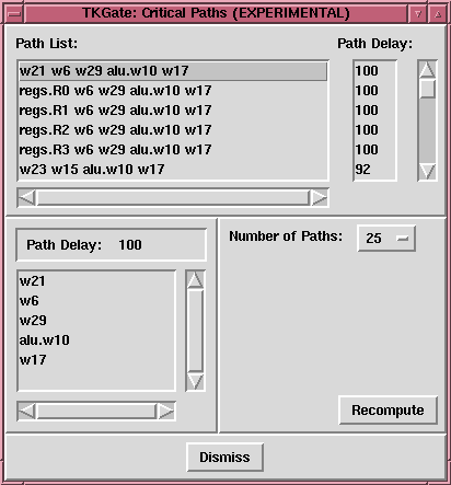
 To invoke the analyzer, click the critical path analysis button on the
right side of the tool bar, or select "Critical Path..." from the
"Circuit" menu. A dialog box like the one shown to the right with a
list of top critical paths and their delays will appear. You can
select a path to display by clicking on it in the listbox. The
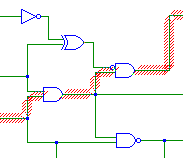
selected path will be shown in the edit window with red hashes as
shown in the figure on the left.
To invoke the analyzer, click the critical path analysis button on the
right side of the tool bar, or select "Critical Path..." from the
"Circuit" menu. A dialog box like the one shown to the right with a
list of top critical paths and their delays will appear. You can
select a path to display by clicking on it in the listbox. The
selected path will be shown in the edit window with red hashes as
shown in the figure on the left.
The lower portion of the dialog box contains a list of the nets on the
currently selected path. By clicking on a net name, the editor will
go to the module with the selected net and highlight it with an "X"
mark. The number of paths to by displayed can be selected with the
selector in the lower right corner. Change this number and click on the
"Recompute" button to change the number of displayed paths.
If you click on a net while in critical path analysis mode, a small
window will appear next to the cursor with a message such as "10 -> w3
-> 50". This means that the selected net is "w3", the worst case
delay from an input to w3 is 10, and the worst case delay from w3 to
an output is 50.
To print a critial path, simply print the circuit while the path is
highlighted.
Last edit by hansen on Thu Sep 21 10:00:28 2000